K-Display 2026, Seoul | Filmed and photographed on site by LUMORA | August 2026
Introduction: reading a display booth like a chemist
K-Display, organized under the Korea Information Display Society, is the annual moment when Korea’s display industry shows where it is going. At the 2026 edition in Seoul, we spent a full day inside the Samsung Display booth with cameras and a materials chemist’s eye. Exhibits like these are usually described in product language: brighter, sharper, faster, more private. Underneath every one of those words sits a molecule, a stack architecture, a purification specification or a deposition process. The purpose of this highlight is to connect what visitors saw on the floor to the materials science that makes each demonstration possible, and to place it all in the larger story of how OLED emitters have evolved over four generations.
Four exhibits organized the booth: Partial Privacy, an OLED whose viewing angle is controlled pixel by pixel; the Edge Device zone, where small OLEDs become the face of AI hardware; QD-OLED with Synchroma, quantum dot color conversion presented as a single consistent color experience across every panel size; and the Digital Cockpit, automotive OLED in its most integrated form yet. Each one rewards a closer, materials level look.
Partial Privacy: viewing angle becomes a pixel property
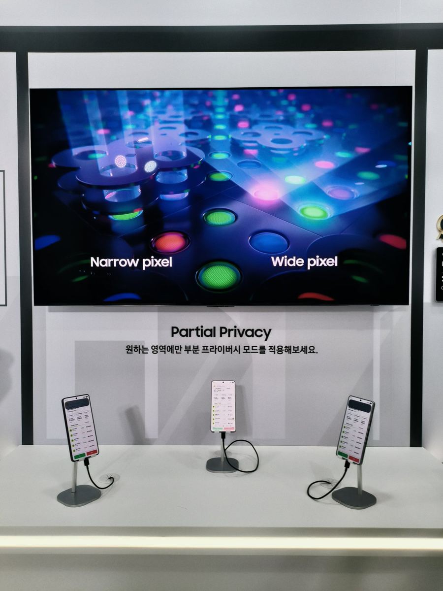
A conventional privacy screen is a micro louver film laminated on top of a finished display. It works like a set of microscopic window blinds that physically block light at oblique angles. The protection is real but the costs are permanent: the film absorbs roughly 30 to 40 percent of the on-axis luminance, the entire screen is affected uniformly, and the user cannot switch it off when sitting alone at home. Every laptop user who has squinted at a dim privacy filtered screen knows the compromise.
Samsung Display’s Partial Privacy demonstration moves the privacy function into the pixel itself. Each pixel can switch between a wide angular emission profile and a narrow one, so privacy becomes an addressable electrical state rather than a laminated compromise. In the booth demo, one region of a smartphone screen, imagine a banking app or a password field, runs in narrow mode while the rest of the display keeps full off-axis readability. Switch it off and the whole panel returns to normal viewing. The privacy performance has been verified by UL, which matters for enterprise buyers who need an auditable claim rather than a marketing one.
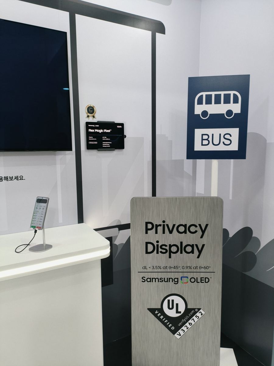
How does a pixel change its emission cone? The answer lives in optics that materials scientists control. The angular emission profile of an OLED is governed by its optical microcavity: the spacing between the reflective anode and the semi transparent cathode, the refractive indices of every organic layer in between, and the exact position of the emission zone within the stack. Change the cavity condition and you redistribute light between forward and oblique angles. Achieving that modulation on command, per pixel, means the pixel architecture can electrically alter where recombination happens or how the cavity resonates. It is a beautiful reminder that hole transport layers, electron transport layers and capping layers, materials that never emit a photon themselves, decide where the photons go. Purity matters here too: transport materials with ppb level metal contamination scatter charge and drift the emission zone over life, degrading exactly the optical precision this feature depends on.
The materials point: privacy mode is cavity engineering. The layers that steer light are as valuable as the layers that make it.
The Edge Device zone: OLED as the face of AI
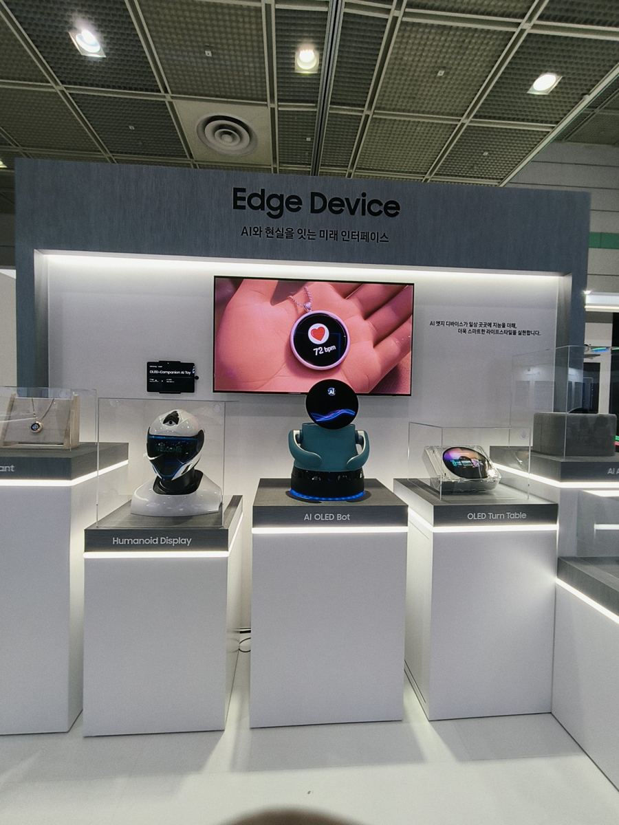
The most photographed corner of the booth collected a family of AI hardware concepts: a humanoid robot whose face is a 6.9 inch OLED with eye tracking, a 1.3 inch circular OLED companion that hangs on a keyring, a pendant that displays the wearer’s heart rate, a pocket sized petbot, and an OLED turntable styled like a speaker. The tagline read, in Korean, an interface for the era when AI meets reality. It is easy to file this zone under charm. The engineering underneath is serious.
These form factors exist because OLED is self emissive. With no backlight unit there is nothing rectangular to preserve, so panels can be cut round or free form. With emission generated in a film stack thinner than a micrometre on a flexible substrate, sub millimetre device profiles are possible. And because a black OLED pixel consumes essentially nothing, an always on companion device can idle for days. Every one of those properties traces to the organic semiconductor stack rather than to any mechanical component.
Always on wearables also stress materials in distinctive ways. Long static images invite differential aging, where heavily used pixels dim faster than their neighbours and leave ghost patterns. Tiny batteries demand maximum efficiency at low luminance, a regime where emitter and host energetics dominate. Skin contact products must manage heat gently. These constraints push directly on emitter chemistry, which is why the emitter generations described later in this document matter well beyond television.
QD-OLED and Synchroma: color purity as a materials specification
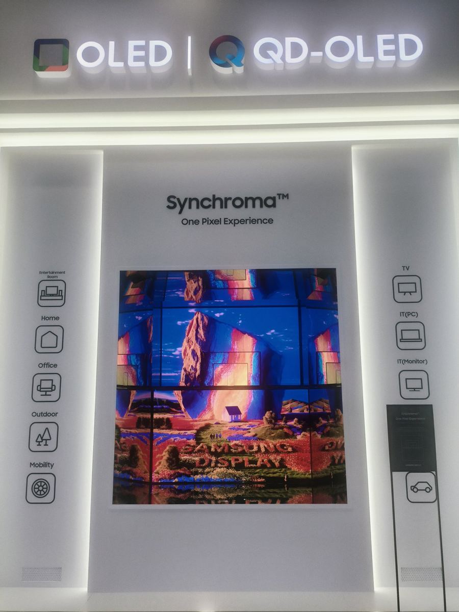
Synchroma is Samsung Display’s name for a consistent color experience across every panel size, from a monitor to a television wall, and QD-OLED is the engine that makes the promise physical. The comparison with LCD explains the idea best. An LCD generates broadband white light behind the panel and then discards most of that spectrum in absorptive color filters to produce red, green and blue. QD-OLED inverts the logic: it starts from efficient blue OLED emission and converts part of it through red and green quantum dots, nanometre scale semiconductor particles whose emission wavelength is set precisely by particle size.
The key specification is the width of the emission band. Quantum dot emission is narrow, roughly 20 to 30 nm full width at half maximum, FWHM. Narrow emission means the red, green and blue primaries sit close to the spectral locus, the pure color boundary, of the CIE 1931 chromaticity diagram. That geometric fact is what pushes QD-OLED coverage beyond 90 percent of BT.2020, the widest broadcast color gamut standard, where a conventional LCD typically manages around 70 percent. Color purity, in other words, is not a tuning trick applied in software. It is a materials specification: narrow FWHM in, wide gamut out. Exactly the same logic drives the frontier of organic emitter design, where the narrowest MR-TADF molecules now rival quantum dots, as described in the generations section below.
Performance has caught up with purity. The booth showed a 31.5 inch 4K QD-OLED monitor running at 360 Hz, an industry first for that resolution and refresh combination, evidence that the color conversion architecture also supports elite motion performance.
Four generations of OLED emitters: the chemistry behind every number
Every brightness, lifetime and efficiency figure on the show floor traces back to one question: how does the emitting molecule handle excitons? This section is the technical heart of this highlight, because the four generations of emitter chemistry are the reason displays look the way they do, and the reason the next displays will look better.
First generation, fluorescence (1987). The modern OLED began with Ching W. Tang and Steven VanSlyke at Kodak, who built the first efficient bilayer organic light emitting diode using the aluminium complex Alq3. When electrons and holes recombine in an organic semiconductor, quantum spin statistics dictate that only 25 percent of the excitons form as singlets while 75 percent form as triplets. A fluorescent emitter can use only the singlets, so its internal quantum efficiency, IQE, is capped at 25 percent. Remarkably, almost four decades later, the deep blue pixel in most commercial OLED panels still runs on this first generation physics. That single fact explains a large share of the display industry roadmap, because blue is the color that limits panel brightness, lifetime and power consumption.
Second generation, phosphorescence (1998). Marc Baldo, Mark Thompson and Stephen Forrest showed that organometallic complexes of heavy metals, first platinum porphyrins and soon after iridium complexes, exploit strong spin orbit coupling to emit light directly from the triplet state. Suddenly all 100 percent of excitons could be harvested. Phosphorescent red and green emitters became the commercial standard and have held it for two decades. The missing piece is blue: a phosphorescent blue with deep color and competitive lifetime has been one of the most valuable unsolved problems in materials chemistry, and the industry watches every announcement in this space closely.
Third generation, thermally activated delayed fluorescence, TADF (2012). Chihaya Adachi and coworkers demonstrated that purely organic molecules, designed with a very small energy gap between their singlet and triplet states, can recycle triplets back into emissive singlets through reverse intersystem crossing driven by ambient thermal energy. TADF offers up to 100 percent IQE without iridium or platinum, which matters for cost, for supply chains, and for molecular design freedom.
Fourth generation, MR-TADF and hyperfluorescence (2016 onward). Takuji Hatakeyama introduced the DABNA family, rigid frameworks of boron and nitrogen atoms in fused aromatic systems, creating what is now called multi resonance TADF, MR-TADF. Their rigidity suppresses the structural relaxation that broadens emission, so they emit with a full width at half maximum, FWHM, near 20 to 30 nm, as narrow as a quantum dot. In a hyperfluorescence device a TADF sensitizer harvests all the excitons and transfers the energy to an MR-TADF terminal emitter, combining complete exciton harvesting with exceptional color purity. This architecture is the emitter community’s road to the BT.2020 color standard, and it is the chemistry LUMORA works with every day.
Read the booth through this lens and it resolves into materials statements. QD-OLED achieves its gamut through narrowband quantum dot emission, while its blue pump layer is exactly where fluorescent efficiency limits still bite. The Edge Device concepts depend on efficiency at low luminance, an emitter property. Which makes blue emitter chemistry, whether phosphorescent, TADF or hyperfluorescent, the single highest leverage materials problem in the display industry today.
Digital Cockpit: where lifetime beats efficiency
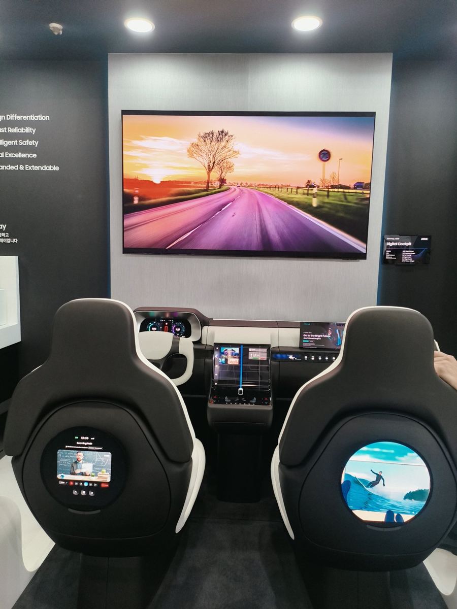
The automotive zone assembled a complete cockpit. A cluster display faces the driver. A slidable centre display extends to 15.5 inches on demand and retracts when not needed. Round OLEDs sit in the seat backs for rear passengers. Most striking to a process eye is hole in active area technology, which opens an 80 mm aperture inside a working display so that a physical gear dial and an air vent live surrounded by live pixels. The wall text summarized the design targets: design differentiation, robust reliability, intelligent safety, optical excellence, expanded and extendable.
Automotive is the hardest qualification an OLED material ever faces. A dashboard panel must survive wide thermal swings, direct sunlight loads, and tens of thousands of operating hours, all without differential aging between colors that would make a speedometer slowly discolor. Elevated temperature accelerates every degradation pathway in the emissive layer, so bond dissociation energies, host guest energy alignment, and film purity decide which materials pass. Trace metal impurities at parts per billion levels measurably shorten operational lifetime, which is why sublimation grade purification is the automotive standard. In this market, emitter lifetime, not peak efficiency, is the figure of merit that wins contracts.
The takeaway
Samsung Display’s K-Display 2026 booth read like a map of where OLED materials are going. Light is being steered per pixel by cavity design. Color is being set by narrowband emission, from quantum dots today and narrowband organic emitters next. Form factors are being freed by self emission. Automotive lifetimes are being won by molecular stability and purity. Every headline feature was, underneath, a chemistry result, and the companies that master the underlying materials will define the next decade of displays.
Watch the companion videos: youtu.be/J-t19hHsJ4Q (English), youtu.be/vFx-8xh5VVU (Korean), youtu.be/YoVhQLx3dHA (44 second booth tour).
Glossary for the general reader
OLED. Organic light emitting diode. A display pixel made of thin organic semiconductor films that emit light directly when current flows, with no backlight.
IQE and EQE. Internal and external quantum efficiency. IQE counts photons generated per injected electron inside the device; EQE counts photons that actually escape into the air, typically 20 to 30 percent of IQE without special outcoupling.
Singlet and triplet excitons. The two spin states formed when electrons and holes meet, in a fixed 25 to 75 ratio. Which of them a molecule can use for light defines its emitter generation.
FWHM. Full width at half maximum, the width of an emission peak. Narrower emission means purer color; 20 to 30 nm is the current gold standard for both quantum dots and MR-TADF emitters.
CIE 1931 and BT.2020. The standard map of human color perception, and the widest broadcast color gamut defined on it. Covering more of BT.2020 requires primaries with narrow FWHM.
Tandem stack and charge generation layer. An architecture that stacks two or more emitting units in series, joined by charge generation layers that supply electrons and holes to each unit, trading a little voltage for large gains in brightness and lifetime.
LTPO. A backplane combining polysilicon drive transistors with oxide switching transistors, letting a panel drop its refresh rate on static content to save power.
Nit. One candela per square metre, the standard unit of display brightness. A phone peaks near 1,000 to 2,000 nits; the panels in this report reach 4,500.
MR-TADF and hyperfluorescence. Multi resonance TADF emitters are rigid boron nitrogen molecules with very narrow emission; hyperfluorescence pairs them with a TADF sensitizer that harvests all excitons for them.
Sublimation purification. Purifying a material by evaporating and recondensing it under vacuum, the standard route to the parts per billion purity levels that long lived OLED devices require.
Sourcing the materials behind this story
LUMORA, research to pilot quantities. LUMORA, a brand of LUMORA · a brand of LAMKO Co., Ltd., supplies high purity sublimed OLED, OPV and semiconductor materials, including emitters, hosts and charge transport materials, for research and development use. Every lot ships with a certificate of analysis. Browse the catalogue at lumorachemicals.com or write to sales@lumorachemicals.com.
LAMKO, scale up and CRDMO. For kilogram to production scale supply, custom synthesis of new emitters, and full CRDMO support from first gram to production volume, work with LAMKO. Projects proceed NDA first and your intellectual property stays yours. Start by describing your project to LUMI, our AI project workspace, at lamko.co.kr/lumi, or visit lamko.co.kr.
References and sources
C. W. Tang, S. A. VanSlyke, Applied Physics Letters 51, 913 (1987). M. A. Baldo, M. E. Thompson, S. R. Forrest et al., Nature 395, 151 (1998). H. Uoyama, C. Adachi et al., Nature 492, 234 (2012). T. Hatakeyama et al., Advanced Materials 28, 2777 (2016). Product and exhibit information: Samsung Display newsroom and UBI Research coverage of K-Display 2026 (en.ubiresearchnet.com). All photographs and footage in this document were taken by LUMORA at K-Display 2026.
Disclaimer: this document is educational commentary based on our own visit to K-Display 2026 and on publicly available information. All product names, brands and trademarks belong to their respective owners. No affiliation or endorsement is implied. Specifications quoted are as presented by the exhibitors and may change.
Emitters, hosts and transport layers
We supply high-purity OLED materials in sublimed grades, from grams to kilograms, shipped worldwide.
Visit LUMORA →Kilogram to production, and custom synthesis
For large-scale supply, new material development and CRDMO support, work with LAMKO directly.
Open LUMI workspace →Partner with us